Newsletter - April 5, 2023

Smart Material Solutions continues to grow! In the last nine months, we’ve made a significant breakthrough in our efforts to fabricate large-area metamaterials for the Army, demonstrated a unique structure to enhance the performance of flexible solar panels, and found our work on the cover of ACS Applied Materials and Interfaces

Our industrial partnerships are expanding alongside our federally funded research, and we’re steadily growing our team of employees and partners along with our portfolio of IP. In the past year, a greater percentage of our funding has come from the private sector than ever before. 

Metamaterial fabrication enabled by cylindrical photomasks

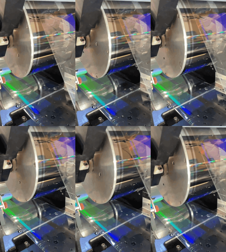
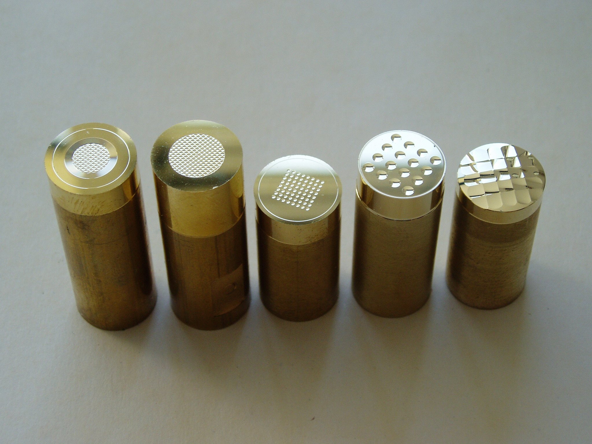
Metamaterial fabrication involves structuring a material to give it valuable properties beyond those of the bulk material. To this end, we recently fabricated a seamless, cylindrical photomask for roll-to-roll (R2R) photolithography to create plasmonic metamaterials with nanoscale patterns that give rise to extraordinary optical properties.

The images below show a photo of a 6-inch diameter seamlessly patterned cylindrical photomask (A), an optical microscopy image with light transmitting through the photomask’s holes (B), and an SEM image of a polymer replica of the mold’s surface (C). SMS partner MicroContinuum, Inc. will soon use this mold to pattern a plasmonic metamaterial absorber film for our Phase II SBIR project with the Army. 

The US Army SBIR office invited our team to submit a Sequential Phase II STTR proposal to continue this exciting work. We proposed creating a series of large-area infrared metamaterials for testing with MicroContinuum and Professor Mark Mirotznik’s group at the University of Delaware.

Self-cleaning, light-trapping nanopatterned coatings for solar panels

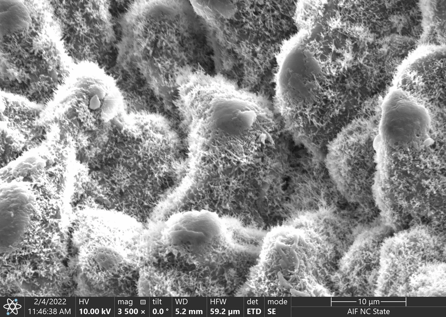
As winners of the Army’s XTech Clean Tech competition, we were awarded a Phase I SBIR to add light-trapping, self-cleaning coatings to solar panels. Our unique hierarchical pattern combines nanoscale moth-eye features and microlenses to both increase power output of the solar panel and prevent the buildup of dust, dirt, and grime that can block incoming light. 

The figure below shows SEM of the hierarchical pattern (A), SEM of a seam between a smooth (left) and a hierarchical (right) pattern with substantially more dust adhered to the smooth film (B), and the short-circuit current of two prototype solar cells in outdoor conditions. The solar cell with a hierarchical coating (left) produces more current than the cell without a coating (right). We’re now working on a Phase II SBIR proposal with MicroContinuum, Inc. and PowerFilm, Inc.

Cover article on dust-mitigating surfaces

Our NASA-funded work on dust-mitigating surfaces with Professor Chih-Hao Chang’s group at UT Austin was recently featured in a cover article in ACS Applied Materials & Interfaces. This paper discusses how our nanopatterns can decrease the adhesion of Lunar dust by over 90% compared to smooth surfaces of the same material.

Other Announcements

Antimicrobial Surfaces: Battling Bacteria on the Nanoscale

Germs are everywhere, including where we least want them. Bacteria can easily cause serious disease when they make their way onto medical equipment such as implants and catheters, or even when they are just sitting on surfaces such as door knobs and buttons. The  most obvious solution is to apply antibacterial agents like bleach, iodine, or antibiotic drugs to kill all of the germs. These agents, however, can be almost as unhealthy for us as they are for the germs. Additionally, they can pollute the local environment, be that the tissue around a hip implant or the water reservoir for nearby towns and cities. Lastly, owing to the emergence of drug-resistant “super bacteria,” there is a need for effective approaches that avoid antibiotics; antibiotics will never be able to kill every germ, and the ones that survive become more and more resistant to antibacterial agents. The solution requires antibacterial surfaces that don’t use antibiotics or other toxic chemical agents.

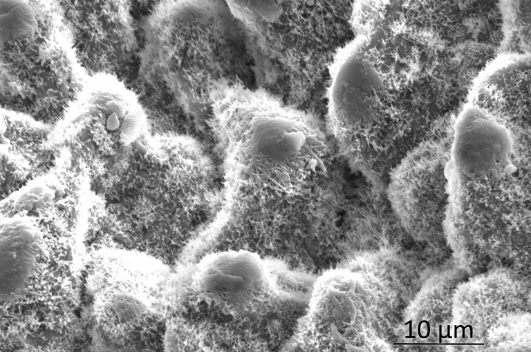
Nature already offers insights towards a solution, as exhibited by superhydrophobic lotus leaves or anti-reflective moth’s eyes. Surfaces with natural antibacterial properties can be found in, or rather, on sharks and cicadas. Close inspection reveals why: scanning electron microscopy (SEM) images taken at NCSU’s Analytical Instrumentation Facility shows that these surfaces are covered with nanoscale features (Figure 1). The microstructures on the shark’s skin prevent bacteria from adhering to the surface, making the surface “anti-fouling.” This is why you never see a shark covered in algae, while turtles are often covered in an undesirable layer of slime. Through a deadlier effect, the nanopillars on cicada wings may puncture and inactivate bacteria, making their surfaces “biocidal.” 

Figure 1: Cicada wings. Photo of a cicada (left) and SEM image of one of its wings (right).

Two categories of antimicrobial surfaces

These two effects of surface structures - anti-fouling and biocidal - present an alternative to the chemical and pharmaceutical attacks of antimicrobial agents (Figure 2). While an anti-fouling surface prevents colonization and formation of a biofilm that leads to further infection, it does not necessarily kill the bacteria. A biocidal surface kills the microbe, but high volumes of debris buildup may cause other issues. 

Figure 2: Types of surfaces. (A) Biofilms can build up on normal, flat surfaces. (B) Microfeatures make a surface anti-fouling by preventing bacterial adhesion. (C) Biocidal surfaces use nanofeatures to kill or inactivate bacteria.

Anti-fouling surfaces

Figure 3: Anti-fouling mechanism. Microfeatures reduce contact area to prevent microbes from anchoring.

Anti-fouling surfaces have many applications, one of the largest being in implants. When a biofilm forms on the surface of an implant, it can cause an infection deep within the body. This is the most common reason implants fail. If the surface of the implant can be functionalized so that bacteria does not stick while not killing the healthy cells around it, the rate of implant failure could be drastically decreased.

The efficacy of a patterned surface depends on the scale of its features relative to the microbe. The average size of a bacterial cell is between one and two micrometers. Microbes can easily colonize features that are larger than the microbes themselves due to the abundance of anchor points to which the microbes can attach and grow. However, when the spacing between the pillars is smaller than the bacteria, the bacteria are unable to stick, as illustrated in Figure 3. For this reason, surfaces with feature sizes between 30 nm and 2 µm have demonstrated a decreased propensity for bacterial adhesion. 

In addition, this same scale of microstructures can create superhydrophobic surfaces when formed into a low-surface-energy material. This low surface energy makes adhesion of almost any molecule difficult, and the resulting dry, barren landscape is particularly inhospitable for microbial life.

Biocidal surfaces

Figure 4: Biocidal mechanism. Nanofeatures puncture membranes or cell walls to kill or inactivate bacteria.

Instead of preventing adhesion, biocidal surfaces actively kill bacteria and prevent it from multiplying. Compared to anti-fouling patterns, biocidal patterns are much smaller. These patterns have nanometer scale pitches - substantially smaller than the average bacteria. Researchers speculate that the sharp points at the top of these features can pierce the membrane of the bacteria, while other mechanisms utilize extremely high aspect ratios that can help rupture the cell wall (Figure 4).

A matter of scale

Since these anti-fouling or biocidal effects depend on the scale of the structure relative to the microbes, and microbes vary in size, it is possible that the same surface is anti-fouling or biocidal for one microbe, but not for another. Animal cells, for example, are much larger than bacterial cells, which is why they are not affected in the same way. For animal cells, nanopatterns can be used on implants to actually help cell proliferation on tissue engineered scaffolds. The nanopatterned surface helps mimic the natural environment that cells typically grow in, allowing them to receive similar signals from their environment.   

What SMS Can Do

Smart Material Solutions’ unique patterning technologies can produce highly customizable surface topographies on a variety of materials, including polymers, that could be optimized for anti-fouling or biocidal properties. By producing drum molds for roll-to-roll nanoimprint lithography, we enable large-scale production for medical equipment or industrial applications. SMS currently collaborates with Professor Roger Narayan at the UNC/NC State Joint Department of Biomedical Engineering to study the antimicrobial properties of some of the patterns we have created.

Improving Solar Panels with Nanotechnology

Additional Author: Brenna Tryon

What is a solar panel?

Figure 1: Dust, dirt, and pollen on solar panels can block incoming sunlight. Any light that is blocked or reflected cannot be absorbed by a solar panel and converted into electrical power.

Solar panels capture sunlight and convert it into electricity that can power our houses and cars. The more light a panel absorbs, the more electrical power it can produce. Ideally, a solar panel will absorb all incident sunlight, rendering it completely black. To do this, all incoming light must enter the panel and be trapped there until it is completely absorbed. In reality, some light is not absorbed because it reflects off the panel, is blocked by particles like dirt, or escapes the panel before being absorbed (Figure 1).

Nanoscale features such as moth-eye coatings, light-trapping features, and plasmonic structures can reduce reflections and confine light inside the solar panel so that more light is absorbed and converted into electricity. Many of these nanopatterns also act as self-cleaning or dust-mitigating surfaces that prevent the buildup of dust, dirt, and pollen that can block incoming light and decrease efficiency.

Moth-eye features decrease reflections

Moth-eye features are modeled after the nanofeatures that make moths’ eyes anti-reflective. Moth-eye coatings have nanofeatures that are smaller than the wavelength of light. Their small size makes moth-eye features anti-reflective by tricking light into believing that the transition from air into the solar panel is a gradual change rather than an abrupt interface.

Moth-eye features reduce the amount of light reflected from the surface of the solar panel, as illustrated in Figure 2. Theoretically, perfect moth-eye features can completely eliminate the Fresnel reflection off the top surface, allowing 100% of the incident light to enter the panel. Unfortunately, this same phenomenon will also allow light that has traveled through the panel to escape more easily. As a result, anti-reflective coatings such as moth-eye nanofeatures are often combined with light-trapping microfeatures that confine light inside the solar panel.

Figure 2: Illustration of light interacting with a solar panel without (A) and with (B) a moth-eye coating. Incoming and reflected light are shown in yellow and orange, respectively.

Light-trapping features increase absorption

Light-trapping features redirect light to increase its chance of being absorbed by a solar panel. These microscale features are larger than moth-eye nanofeatures and redirect light according to ray optics – the same physics that describes how a camera lens focuses light. Properly designed light-trapping microfeatures increase the amount of light a solar panel absorbs by increasing its path length inside the panel and giving reflected light a second chance at being absorbed.

Optical path length is the distance light travels in a material, in this case the light-absorbing material of a solar panel. Figure 3A shows a solar panel without light-trapping features where the optical path length is slightly more than twice the panel thickness. Light-trapping features like those illustrated in Figure 3B can bend, scatter, or diffract light to increase its optical path length and thus increase its chance of being absorbed by the solar panel. Although Figure 3 shows light-trapping features on top of the solar panel, similar features on the reflective back surface can also scatter light to increase its optical path length. 

If light is scattered to a shallow enough angle, it can undergo total internal reflection so that all the light inside the panel is internally reflected. This enables the light to make multiple passes back and forth inside the panel and creates an optical path length that is many multiples of the panel thickness. For a random texture on the top surface, the Yablonovitch limit predicts a maximum optical path length of about 50 times the panel thickness for silicon solar panels (maximum optical path length for random structures = 4n2(panel thickness) where n is the refractive index of the solar panel). Periodically arranged structures like diffraction gratings and photonic crystals can overcome this limit and achieve even higher optical path lengths due to the excitation of resonances.

Light-trapping features can also increase absorption by capturing reflected light. For example, inverted pyramid features like those illustrated in Figure 3B enable light that is initially reflected to enter the solar cell through an adjacent inverted micropyramid, thus decreasing losses from reflection (indicated by the orange arrows).

Figure 3: Illustration of optical path length in solar cells without (A) and with (B) light-trapping microfeatures. Incoming and reflected light are illustrated in yellow and orange, respectively.

Plasmonic structures redirect and confine light

Plasmonic structures can also scatter light and confine it inside a solar panel, although they function very differently from the light-trapping microfeatures discussed above. Plasmonic structures consist of nanoscale metal structures, often in the form of patterned metal films or metal nanoparticles. These structures manipulate light by causing the electron cloud inside the nanoscale metal to oscillate. These plasmonic structures can be added on the top, middle, or back reflector of a solar panel to scatter light, increase its optical path length, promote total internal reflection, and act as antennas that concentrate light inside the panel. Well-designed plasmonic structures therefore make it easy for light to enter and hard for it to leave a solar panel.

Nanostructures have anti-fouling properties

The buildup of dirt, dust, grime, and sand that blocks incoming light is a big problem for solar panels. In fact, the buildup of dust on the solar panels of Mars rovers often reduces available power or temporarily shuts them down until Martian windstorms blow away the dust, reviving the rovers’ solar panels. On Earth, cleaning is often needed, especially in desert environments that lack rainfall.

Figure 4: Video showing how a nanopatterned surface (right) exhibits significantly less dust adhesion than a smooth surface of the same material (left).

Fortunately, many moth-eye and light-trapping nano- and microfeatures also make surfaces dust mitigating and anti fouling. The lotus effect, named for the nanoscale features that make lotus leaves self cleaning, decreases particle adhesion to a surface by decreasing the contact area. Nanostructures can also make surfaces superhydrophobic, making it easier for rain to wash away any particles that do buildup.

Smart Material Solutions, Inc. and Professor Chih-Hao Chang’s group at UT Austin recently created nanopatterns that significantly decrease the adhesion of Lunar dust for a NASA-funded project (Figure 4). This is great news for solar panels both in space and on Earth!

Solar research at Smart Material Solutions

Smart Material Solutions, Inc. (SMS) recently won the Army XTech Clean Tech Competition and a Phase I Small Business Innovation Research (SBIR) grant to use nanocoining and R2R NIL to manufacture light-trapping, self-cleaning coatings that increase the efficiency and reliability of thin-film solar panels. Thin-film solar panels can be lightweight and flexible, making them easy to transport and deploy. SMS will increase the performance of these solar panels by adding nanopatterns like those shown in Figure 5 to solar panels and demonstrating their light-trapping and anti-fouling properties. After the creation of prototypes in Phase I, SMS plans to partner with a solar company to roll-to-roll manufacture panels with self-cleaning, light-trapping coatings during Phase II of the project.

Figure 5: Light-trapping microfeatures patterned in polymer using nanocoining and nanoimprint lithography at SMS include pyramids, inverted pyramids, microlens arrays, and hierarchical features with nanofeatures on top of microfeatures. SEM images taken by Lauren Micklow and Brenna Tryon at the Analytical Instrumentation Facility (AIF).

The “moth-eye” effect: how tiny surface textures suppress reflections and capture light

Light changes when going from one transparent medium, like air, into another, like water or glass. This is evident from the distorted images we see while looking through the water in a pool or from the magnifying effect of a glass telescope, microscope, or camera lens. 

Figure 1: Fresnel reflections are distracting on a glass window (above) or display screen and wasteful on the cover of a solar panel.

These effects occur because different materials have different refractive indices. Refractive index is a measure of how fast light moves through a material. The larger a material’s refractive index, the slower light travels through it. When the light moves from one material into another, e.g. air into glass, there is an abrupt change in refractive index. The light suddenly slows down as it enters the glass, causing some of the light to be reflected. This reflection is called a Fresnel reflection (Figure 1). We observe Fresnel reflections everyday when we see our own reflection in a window at night or glare on the screen of our smartphone. Moth-eye structures can help eliminate these reflections.

Nature’s inspiration - a matter of life and death

Moths are pretty defenseless creatures, and as creatures of the night, they rely on camouflage and stealth to survive. For many animals, the only way we can spot them at night is by the Fresnel reflections off their beady eyes. However, moths have evolved their own solution to prevent these unwanted reflections - billions of tiny nanofeatures on their eyes that not only suppress Fresnel reflection, but also draw that light into their eyes, improving the moth’s vision in the dark. 

To get a better look at these anti-reflective nanofeatures, we took the Atlas moth shown in Figure 2 to a scanning electron microscope (SEM) at NCSU’s Analytical Instrumentation Facility (AIF). The SEM images revealed microscale hexagons covered with the nanofeatures that make the eyes anti-reflective. Scientists have attempted to mimic these nanofeatures to create so-called moth-eye anti-reflective coatings for products ranging from televisions and displays to solar panels. For solar panels, moth-eye coatings can increase light absorption and efficiency.

Figure 2: Photo of an Atlas moth with SEM images of one of its eyes.

How Nanopatterns Reduce Reflections

The nanoscale bumps of a moth’s eye make them anti-reflective by altering the effective refractive index at the interface between air and the eye. Let’s consider the analogous case of light traveling from air into glass as illustrated in Figure 3. Air has a refractive index of 1, whereas glass has a refractive index of 1.5. This means that light travels faster in air than in glass, and the abrupt change in speed across a smooth interface causes the Fresnel reflection, Figure 3A.

The key to the anti-reflective behavior of moth eyes is the nanofeatures that are extremely small – much smaller than the wavelength of visible light. Thus, the light cannot resolve the nanofeatures just as we cannot see the tiny water droplets that make up a cloud. Instead of observing the individual nanofeatures, the light observes an average of the nanofeatures and the air. The light therefore experiences a gradual change in the refractive index instead of the abrupt change at a smooth interface, Figure 3B. As a result, the light gradually slows down and the amount of light reflected is reduced. Not surprisingly, the size and shape of the features matter! We studied the effects with partners at the University of Delaware during an Army-funded SBIR project and published the results in JOSA-B.

Figure 3: Illustration of the effective refractive index as a function of position for a smooth interface (A) and a moth-eye structure (B).

Replicating Nature’s Design

Figure 4: Metal mold shim created by SMS with textured and smooth sections (left) alongside a polymer replica showing reduced glare in the textured region (right).

Figure 4 shows how we have been able replicate this effect on a piece of clear plastic at Smart Material Solutions (SMS). The metal mold on the left was partially textured using SMS’s patented nanocoining process. In the polymer replica on the right, the textured region appears transparent, while the smooth region, although completely clear, has so much reflective glare that we can hardly see through it. The man-made moth-eye texture suppresses reflection, and in doing so, actually increases how much light goes through the plastic film.

Moth-eye coatings have several benefits over traditional anti-reflective coatings such as quarter-wave films or multiple graded index films. Moth-eye coatings exhibit broadband, wide-angle anti-reflectivity, meaning that they work for a wide range of wavelengths (colors) and angles of the incoming light. In addition, the moth-eye nanofeatures can also make a surface self-cleaning or superhydrophobic, critical properties for applications including solar cells, lenses, and windows, where the buildup of dirt, dust, pollen, and grime can substantially degrade performance.

Problems and Solutions

Unfortunately, in addition to their promises to enhance solar panel efficiency and create self-cleaning, glare-free display screens, nanofeatures also inspire trepidation in engineers, who time and again find themselves facing the same problems: these textures are easily damaged by touch, easily contaminated by fingerprints, and extremely difficult to fabricate in a cost-effective way. 

However, these problems are gradually being solved. Durability and contamination issues can be somewhat mitigated by new polymer formulations with low surface energy and exceptional hardness. In the meantime, SMS is focused on applications that are low touch or can tolerate some defects, such as solar cells. 

And the problem of fabrication at scale is SMS’s specialty. We recently worked with MicroContinuum, which used a seamless mold created by SMS’s core technology nanocoining, along with roll-to-roll nanoimprint lithography (R2R NIL) to nanopattern over 500 feet of motheye film, Figure 5. It’s a multifaceted engineering challenge, but over time Smart Material Solutions will help bring these enormous benefits into the consumer world. 

Figure 5: Photo (A) and SEM (B) of a piece of the over 500 feet of moth-eye film embossed at MicroContinuum, Inc. This moth-eye film has nanofeatures with a pitch of 300 nm that induce blue and green diffraction at low viewing angles and anti-reflective properties at normal angles.

Author: Stephen Furst
Contributor: Brenna Tryon

SEM Gallery: Images from Our Work at the Nanoscale

The following is a collection of scanning electron micrographs taken as a part of ongoing research initiatives at SMS. They highlight patterns that are being developed for active projects and internal research as well as relevant patterns found in nature.


Molds

Metal molds created using our seamless nanopatterning process, nanocoining.

Ripples in the diamond die were replicated into the electroformed copper mold

Ripples in the diamond die were also replicated into the high phosphorous nickel mold

Material flow resulting from the nanocoining indenting process

Close up of material flow due to indenting


Polymer Replicas

Following the fabrication of a master mold, the pattern can be transferred using nanofabrication techniques including thermal embossing and nanoimprint lithography.


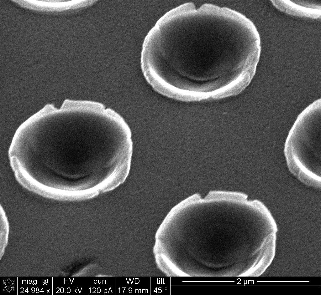
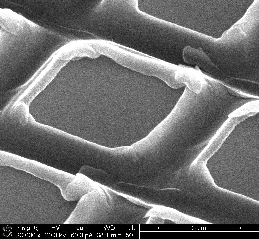
Nanoimprint lithography (NIL) with a mold created with nanocoining at SMS was used to pattern this resist. Subsequent etching steps transferred this pattern into a metal layer to create a metal-mesh film for plasmonic IR absorbers.


Replica Flaws

Wrinkles and bubbles in replicas

A bubble between a UV-cured grid pattern and its polycarbonate backing


Interwoven Indents

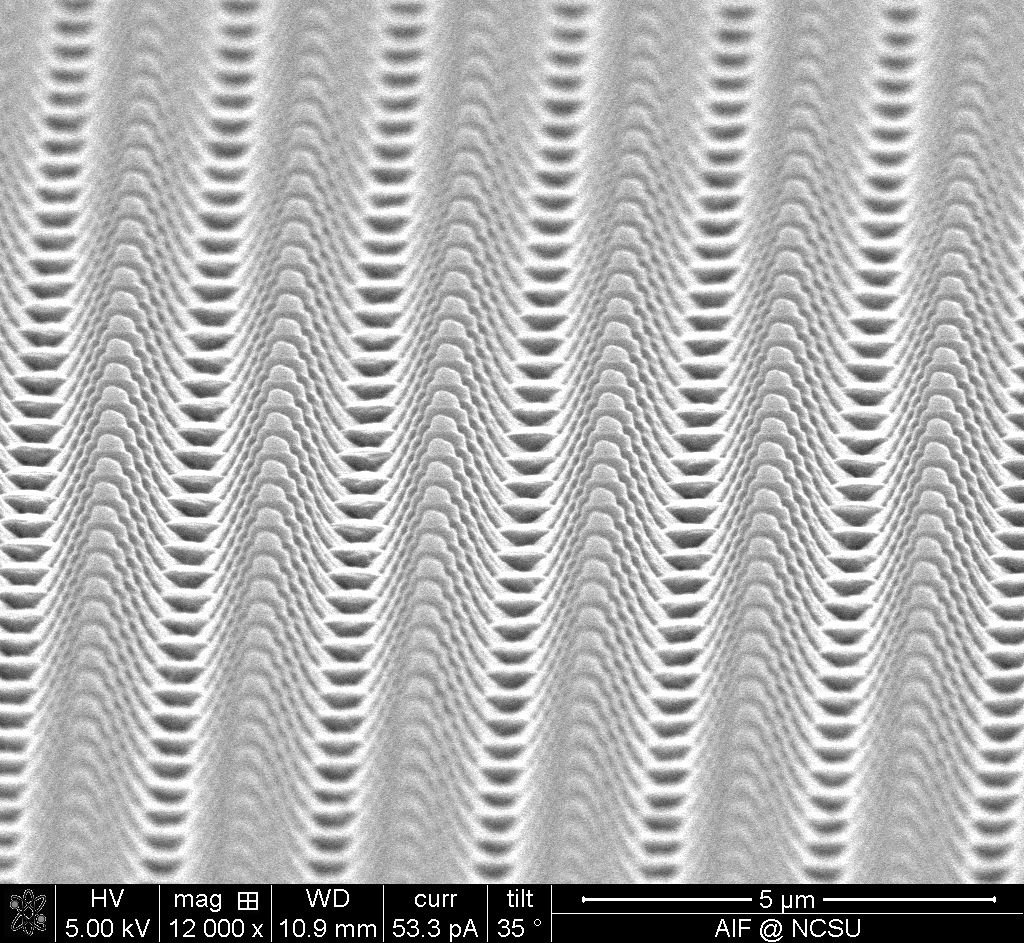
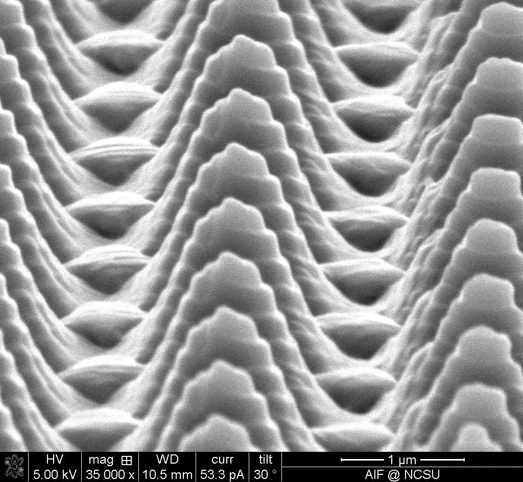
Intentional tiling errors during the nanocoining process create patterns consisting of differently sized features.

A micropattern replicated into a photopolymer using a flexible shim and a batch NIL process

A pattern replicated using one of our seamless sleeves and a UV Roll-to-Roll NIL process


Nature

Many engineered nanopatterns find inspiration from nature. The biomimetic effects include hydrophobicity and structural color.

Intricate hierarchical patterns make lotus leaves self-cleaning and hydrophobic.


The microscopic tree-like structures give Morpho butterfly wings their vibrant blue color through a phenomenon known as structural color This image resembles a forest with tree-covered hills.


These images were taken by Lauren Micklow, Nicky Cates, and Brenna Tryon at the North Carolina State University Analytical Instrumentation Facility using an FEI Quanta 3D DualBeam SEM/FIB or a Helios 5 Hydra DualBeam SEM/pFIB.

Newsletter - June 28, 2022

Who are we, what are we doing, and why?

SMS’s Material Scientist, Dr. Nicky Cates, stopped by the It’s a Material World Podcast to answer these questions, and more. This is also a great listen for any aspiring MSE!

We’ve successfully created a dust-mitigating nanostructure!

The past 6 months have been the best yet for Smart Material Solutions. This included a breakthrough in our efforts to create a Passive Dust-Mitigating surface for NASA through a Phase 1 SBIR Project with Prof. Chih-Hao Chang’s group at UT Austin that concluded in November. 

The result: we created a nanostructured surface that reduced dust coverage by 93% compared to a smooth surface of the same material. The video below shows how a lunar dust simulant slides right off our nanostructured surface, while sticking to a smooth surface of the same material. The SEM image shows a side-angle view of the seam between the structured (right) and smooth (left) regions of the same sample. The division is dramatic, and represents a potential game-changing advance in NASA’s efforts to reduce dust adhesion on critical components, including solar panels, radiators, camera lenses, and spacesuits. Results have been submitted for review in a publication led by Prof. Chang and his student, Samuel Lee.

NASA Phase II SBIR funded

Our success in Phase 1 led to a $750,000 Phase 2 contract to improve surface performance, transfer the patterns into several more space grade materials, demonstrate imprinting roll-to-roll, create application demos, and further understand the physics that drive this phenomenon. We’re partnering once again with UT Austin, who will test our samples in a lunar simulation environment and lead the effort to study particle adhesion physics, along with Microcontinuum, Inc. who will replicate our molds using roll-to-roll nanoimprint lithography.

Application demos will include solar cover glass, visible optics, and radiator films

Army research underway

The US Army has been our biggest supporter, and work continues to use our patterning methods and roll-to-roll processes to create large area anti-reflective surfaces and metamaterials for multiple national defense applications. We’re partnering with the University of Delaware (UD) and Microcontinuum, Inc.. UD Prof. Mark Mirotznik, his graduate student Alex Winters, and the SMS team recently published on the topic in the Journal of the Optical Society of America B.

Microcontinuum imprinted more than 500 linear feet of our anti-reflective motheye film using roll-to-roll NIL.

Our next big pitch: the Army’s XTech Clean Tech competition

Dr. Nicky Cates, our resident solar expert, is leading an effort to pitch our light-trapping and dust-mitigating surfaces to the Army to improve the flexible, thin-film solar panels that power electronics on the battlefield. We’ve crossed the first hurdle, as our white paper was selected for a live pitch next week. If we’re selected, we’ll have a great line on more than $2M in funding to focus on enhancing the performance of thin-film solar cells - one of our most promising application targets.

Diamond Turning: a Single-Step Process to Create Precise Parts with a Reflective Finish

Smart Material Solutions’ novel nanopatterning process - Nanocoining - has a unique origin story within the nanotech world. Unlike most nanopatterned mold-making techniques that require a lithographic techniques like those used to make computer chips, Nanocoining is based on a mechanical indenting process that is derived from diamond turning. 

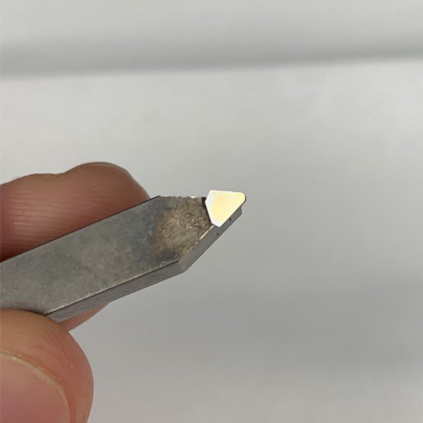
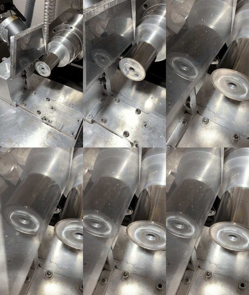
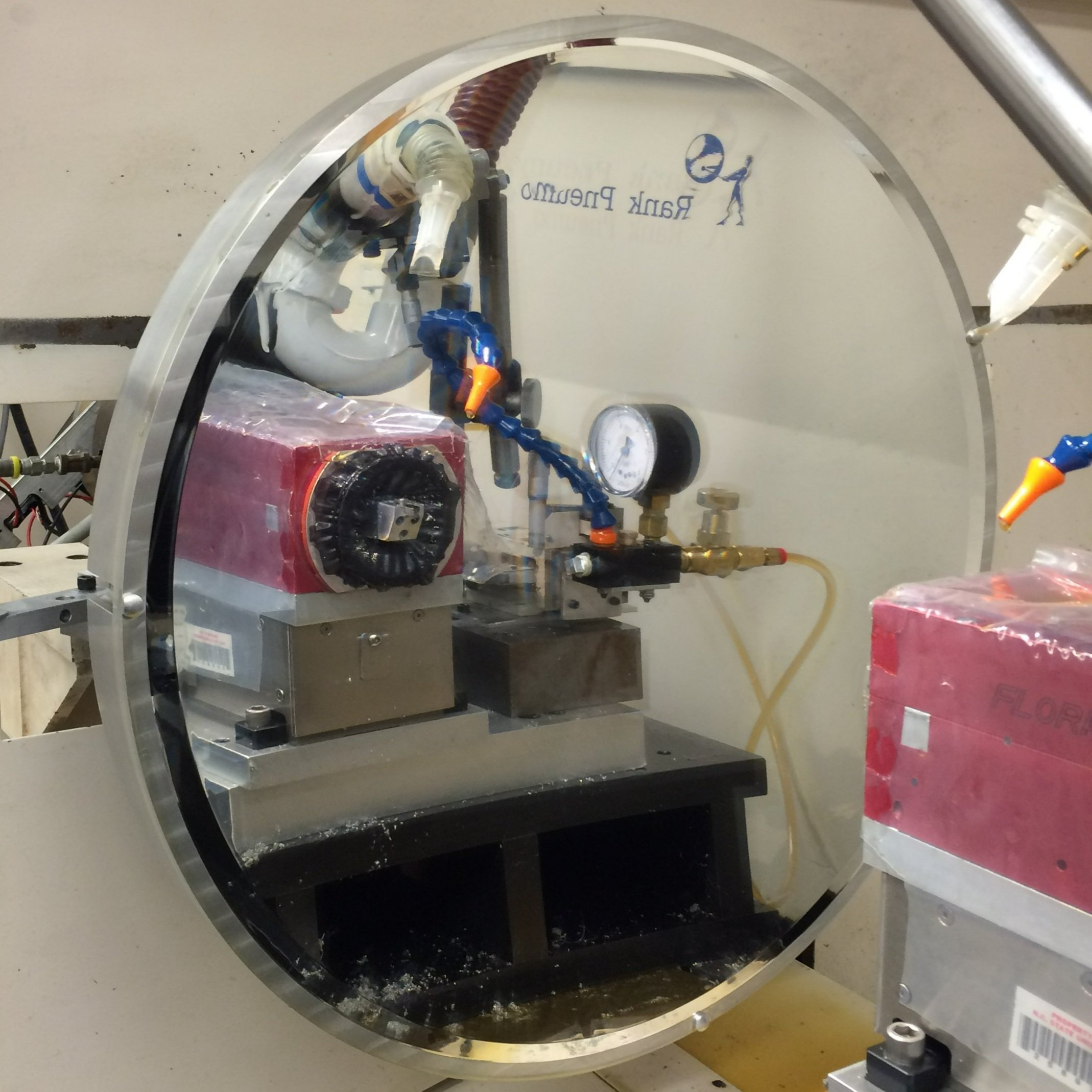
Diamond turning is, simply put, cutting a part on a very precise computer numerical control (CNC) lathe using a sharpened diamond tool. The process involves mounting the part on a spindle that rotates the part (a copper cylinder in the video on the right) while a diamond tool drags across the part’s surface to cut it. The resulting spiral cut around the surface creates a single chip that can be miles long. The diamond tool is so sharp and the CNC axes so precise that diamond turning can simultaneously control both the form (or shape) and surface finish, even for optics that require an extremely smooth mirror finish. Surface roughness as small as 1 nm root mean square (RMS) can be achieved with an air-bearing spindle and air- or oil-bearing linear axes. 

A high-quality optic will have form errors less than one sixteenth of the smallest wavelength of interest, meaning that for visible light (down to 390 nm), form errors have to be less than 25 nm! To produce a mirror-like surface with minimal diffractive effects, the surface finish has to be even better, often less than 3 nm RMS. The ability to produce high-quality surface finish in the cutting step eliminates the need for a polishing process. However, this requires not only an atomically sharp tool and stiff, precise axes, but also careful control of the chip via, for example, a vacuum (video on right) to ensure it does not damage the part. During a good cut, this chip should be a continuous string that is a few micrometers thick and wide, but tens of kilometers long.

A Deterministic Process

Geometry of the grooves formed during a diamond-turning process.

In diamond turning, surface finish is derived primarily from the size of the grooves left by the diamond tool as it cuts a chip from the part. The sketch on the right shows how theoretical kinematic roughness is affected by the tool radius and crossfeed, or how far across the part the tool moves per revolution. Equation (1) gives an approximation for the peak to valley (PV) surface roughness as a function of crossfeed and tool radius. For this geometry, RMS roughness is a third of PV roughness, so a small crossfeed is needed to ensure a high-quality surface finish.

PV roughness =  
crossfeed2
8*tool radius
(1)

Other metrics that affect cut quality include cut speed, depth of cut, and cut distance, which often must be balanced with crossfeed. However, cutting a part with a fine crossfeed increases cut distance, Equation (2), leading to more tool wear and eventually a degradation of surface finish.

cut distance =  
part diameter*π*traverse
crossfeed
(2)
cut speed =  
part diameter*π
spindle RPM
(3)

Fine crossfeeds also add to processing time (cost) and the likelihood of temperature changes affecting the part’s shape. High cut speeds reduce processing time, but increase sliding velocity which increases temperature, and at some point, tool wear. Regardless, so long as these process parameters can be controlled, the same set of inputs should create a repeatable part and metrology can be used to determine errors that can be compensated out. This is known as a deterministic process

Materials and Form Factors

Diamond turning is best suited for cutting non-ferrous materials like aluminum 6061, brass, copper, or electroless or electrolytic coatings, like copper or nickel doped with high concentrations of phosphorous. These electroformed materials are attractive because of their superior hardness, extremely fine grain size, and, ideally, low incidence of impurity. Using these materials along with a proper lubricant, a diamond tool can remain sharp for miles of cut distance - enough to cut a surface with an area greater than a square meter. Ferrous materials like steel are typically avoided because they rapidly wear the diamond tool.

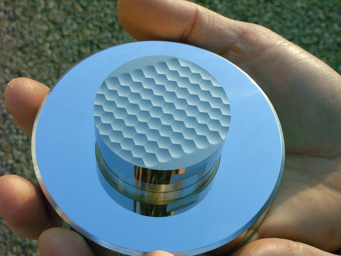
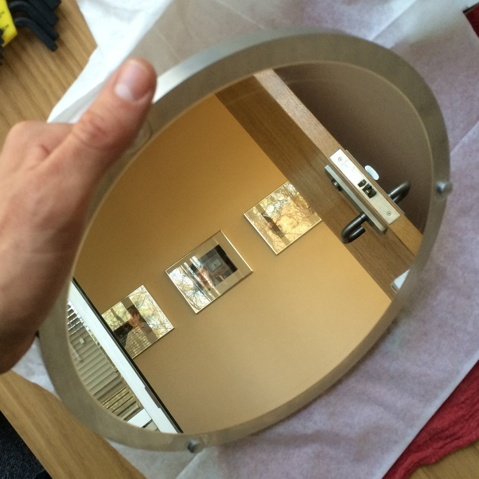
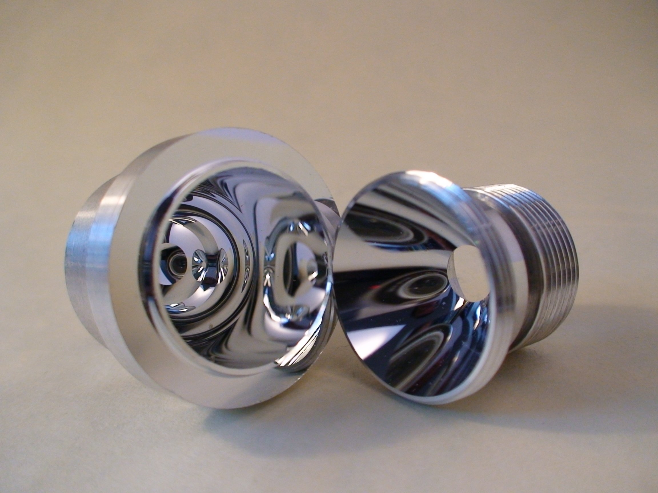
Since diamond turning is done on a lathe, radially symmetric components are easily accessible. This includes cylinders or spherical or parabolic optics. However, the addition of supplemental machine axes such as a Fast Tool Servo that can plunge in and out in sync with the rotating spindle allows for the creation of non-radially symmetric or “free-form” optics. Other methods such as mounting a part off center on the spindle, enables creation of non-radially symmetric conic sections. Photos of both radially and non-radially symmetric diamond-turned parts are shown below.

Nanocoining relies heavily on extremely precise controls processes that are maintained at high speed. However, by borrowing from the deterministic tool kit developed for diamond turning, Smart Material Solutions is able to limit alignment errors and maintain low defect rates, even while tiling billions of indents on a seamless drum mold.

Acknowledgements:

Hydrophobicity: Why Lotus Leaves Fear Water

Many plants and insects exhibit self-cleaning properties as a result of the hydrophobic nature of their leaves and wings. Instead of spreading out on these surfaces, water beads up into a tight ball that minimizes its contact with the surface. This “superhydrophobic” interaction is commonly referred to as the lotus effect because it was first studied in lotus plants. The top of the lotus leaf consists of hierarchical micro- and nanofeatures that enhance the hydrophobicity of the waxy leaf. To demonstrate, I grew a lotus leaf and imaged the surface and its interactions with water droplets, seen in Figure 1. If this natural phenomenon can be harnessed, for example in food safe non-stick coatings, anti-icing surfaces for airplanes, or oil-repellent surfaces for camera lenses, it can improve our everyday lives.

Figure 1. SEM images of SMS's lotus leaf and a photo of the leaf diplaying hydrophobicity

But what causes water to show a fear of the surface and bead up in hydrophobic interactions but spread out readily in hydrophilic ones? The answer lies in both the chemistry and texture of the surfaces. Every surface or interface holds energy due to the broken or dangling bonds searching for a chemical mate. The most stable state of the droplet on the surface is the state that minimizes the area of the high-energy interfaces while maximizing the area of the low-energy interfaces.

When considering a droplet on a solid surface, there are three interface energies to consider: the liquid-vapor, solid-liquid, and solid-vapor interface energies. A simple way to evaluate the interaction between these three values on an untextured surface is Young’s contact angle - the angle of the liquid-vapor interface measured through the droplet. Contact-angle measurements are often used as a measure of the hydrophobicity of a planar surface due to challenges in measuring the surface interactions.

Figure 2. The states of a water droplet on a surface and the associated contact angles.

The solid-liquid interfacial energy ( γsl) can be used to predict changes in Young's contact angle, assuming the solid and vapor remain the same. A high γsl leads to a higher contact angle because the liquid and solid don’t want to be in contact with each other - this causes the water to attempt to find stability elsewhere by creating a bead of water (Figure 2a,b). The inverse is also true - a low γsl leads to a low contact angle as the interface is stable and the liquid and solid want to remain in contact with each other (Figure 2c,d). 

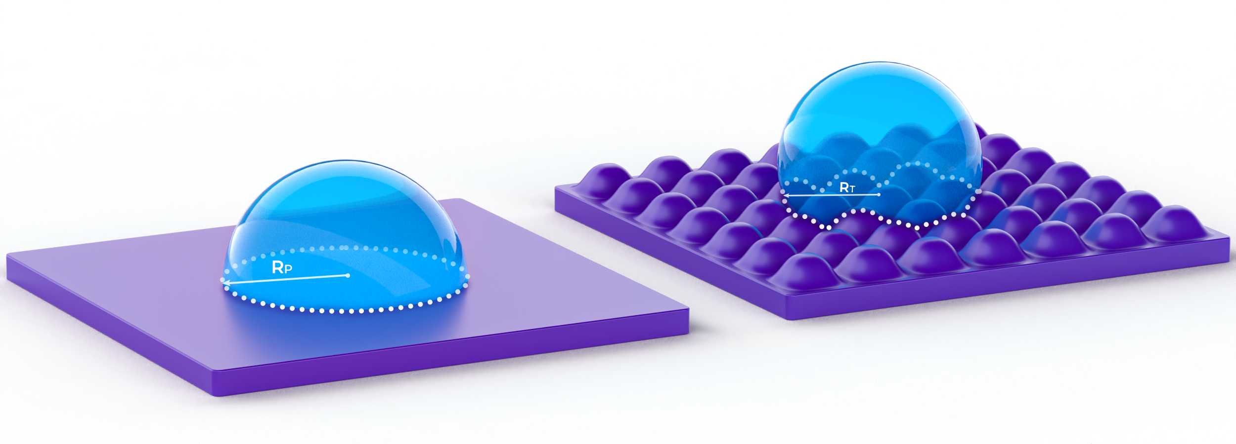
Texturing a surface can enhance the existing interaction between a liquid and a surface - in fact, it is currently only possible to achieve superhydrophobicity with a textured surface. This enhancement occurs because applying a texture increases the surface area and therefore increases the intensity of surface energy on the solid, changing the balance between the three interfaces. Assuming the interaction started hydrophobic, the water droplet will continue wanting to have minimal contact with the solid. The radius of the droplet will shrink from RP on the planar surface to RT on the textured surface, resulting in the enhanced hydrophobic interaction seen in Figure 3.

Figure 3. The hydrophobic enhancement between planar and textured surface. The dashed lines surround the solid-liquid interface of the droplets.

There are two possible states for a droplet on textured surfaces, the Wenzel state and the Cassie-Baxter state (Figure 4). In both states the interaction can be measured via the apparent contact angle (θ*). In the Wenzel state, the droplet has fully wetted the texture; a hydrophobic surface will become more hydrophobic and a hydrophilic surface will become more hydrophilic. In the Cassie-Baxter state, the texture is partially wetted with air trapped between the bottom of the texture and the droplet. Textures with drops in the Cassie-Baxter state always increase the hydrophobicity of hydrophobic surfaces, but may not increase the hydrophilicity of hydrophilic surfaces.

Figure 4. A water droplet on a planar surface, a droplet in the Wenzel State, and a droplet in the Cassie-Baxter state. Note that the droplet reaches the bottom of the texture in the Wenzel state, but air is trapped below the droplet in the Cassie-Baxter state.

Figure 5. Contact angle of water on a patterned vs smooth surface (silane treated polycarbonate).

The hydrophobic surfaces found in nature can be replicated and engineered for individual applications ranging from liquid-repellent fabrics to drag-reduced surfaces. For example, the Kota Research Group at NCSU has worked to create omniphobic fabrics that can be used as chemical shields against almost all contacting liquids. While SMS has not optimized a surface for hydrophobicity, an improvement in the apparent contact angle has been achieved in small experiments with existing replicas (Figure 5).