Structural Color: How peacocks, Morpho butterflies, and stained glass get their colors

An object’s color arises from how it reflects light. Both pigments and microscale surface structures affect how an object reflects light, but they create color in very different ways. Color therefore has two components: pigmented color and structural color.

You’re likely familiar with how pigments create color by absorbing certain wavelengths (or colors) of light. For example, chlorophyll is a pigment that gives plants their color by absorbing all colors except green (Figure 1A). The remaining green light reflects off the plant into our eyes.

Structural color arises from the selective reflection or absorption of certain colors due to light’s interaction with microfeatures like diffraction gratings, photonic crystals, and plasmonic metamaterials (Figure 1B). Structural color is responsible for the vibrant colors of peacock feathers, butterfly wings, opals, and stained glass. Some animals like octopuses and chameleons achieve adaptive camouflage by altering both the pigments and microtextures of their skin. Scientists hope to harness this phenomenon to design microstructures that enhance, shield, or manipulate light for advanced technologies such as radiative cooling and anti-counterfeiting technologies.

Figure 1: Illustrations of pigmented color (A) and structural color (B). Plants are green because the pigment chlorophyll absorbs all colors except green. Morpho butterflies appear blue despite being pigmented brown because the microstructures on their wings selectively reflect blue light. Note that light from the sun includes a mixture of all visible colors.

Diffractive Color

Peacocks and Morpho butterflies get their vibrant colors from a type of structural color known as diffractive color. Diffraction occurs when light interacts with regularly repeating structures, often called diffraction gratings or photonic crystals. The repeating features cause some wavelengths of light to cancel out (destructive interference) while other wavelengths add together (constructive interference), making those colors vibrant. The enhanced color can change with viewing angle, so diffractive materials are often iridescent.

To better understand this phenomenon, we used a scanning electron microscope (SEM) at NC State’s Analytical Instrumentation Facility (AIF) to take a closer look at peacock feathers, Morpho butterfly wings, and one of Smart Material Solution’s roll-to-roll nanoimprint lithography (R2R NIL) molds. Figure 2 shows a photo of a peacock feather and an SEM image of the structures responsible for its bright colors. The butterfly wings in Figure 3 have tree-shaped microstructures that diffract a vibrant blue color that changes little with viewing angle, whereas the micropatterns on the curved surface of the R2R NIL mold in Figure 4 result in a rainbow due to the angle dependence of the diffracted color.

Also at NC State, Professor Michael Dickey’s research group has created switchable diffractive gratings that can be turned on by applying pressure that buckles the surface into regularly repeating microstructures.

Figure 2: Photo and SEM image of a peacock feather.

Figure 3: Photo and SEM images of a Morpho butterfly wing.

Figure 4: Photo and SEM image of a R2R NIL mold created by Smart Material Solutions.

Plasmonic Color

Another type of structural color, known as plasmonic color, is responsible for the brilliant colors of stained glass. But what are plasmons? And how do they give rise to color?

Metals contain electrons that are free to move around the material. These free electrons are known as an electron cloud, a sea of electrons, or an electron plasma. When light waves strike a nanostructured metal, they can create plasmons — or waves in the electron cloud with many electrons vibrating back and forth together. Energy is conserved because some of the light’s energy is transferred into the plasmon. In this way, the nanostructured metal absorbs a certain color of light.

The wavelength of light that is absorbed depends strongly on geometry of the nanostructured metal, so the resulting color can be tuned by changing the size and shape of the metal. The nanoscale metal can take many forms including metal nanoparticles, metal films separated by a nanoscale dielectric cavity, and nanopatterned metal films. In stained glass, suspended lead nanoparticles cause plasmonic absorption and therefore create bright colors.

Large-Area Plasmonic Absorbers

Smart Material Solutions is collaborating with MicroContinuum, Inc. and Professor Mark Mirotznik’s lab at the University of Delaware to fabricate large-area tunable infrared plasmonic absorbers. This project, which is funded by a Phase II Army SBIR grant, uses plasmonic metal-dielectric-metal (MDM) stacks to create tuned absorption. These plasmonic MDM stacks combine the resonance of the dielectric cavity with that of the plasmonic top layer to create strong, tunable absorption. In the phase I project, we fabricated the plasmonic absorber shown in Figure 5 using scalable processes such as nanocoining and nanoimprint lithography (NIL). The phase II project focuses on the roll-to-roll (R2R) nanofabrication of at least one square meter of a plasmonic metamaterial.

Figure 5: Photo and SEM image of a 150 mm x 150 mm plasmonic absorber with a micropatterned metal mesh fabricated during the phase I project.

Roll-to-Roll Nanoimprint Lithography to Add Function to Surfaces

Roll-to-roll, also referred to as reel to reel, technology began in the 1800’s as a way to mass produce newspapers and photographs. Since then it has been incorporated into the production of goods ranging from food packaging to flexible electronics, and more recently in emerging nanotechnology applications. Smart Material Solutions primary mission is to supply the seamless nanopatterned drum molds needed for roll-to-roll nanoimprint lithography (R2R NIL).

R2R manufacturing is a method of fabrication in which a continuously moving, flexible substrate is processed. The processing looks different depending on the application but can include printing, patterning, coating, or lamination. In all cases, the substrate starts wound on one roll, undergoes the processing steps, and then the finished product is wound onto a second roll (Figure 1). Nanoimprint lithography (NIL) is the process of replicating nanoscale patterns from a mold into another material. When combined, R2R processing and NIL result in a high-speed, continuous process to produce large areas of nanopatterned surfaces.

Figure 1. R2R production diagram, where the processing steps are represented by block S1 through S5 and a tensioning step is represented by roller T.

Figure 1. R2R production diagram, where the processing steps are represented by block S1 through S5 and a tensioning step is represented by roller T.

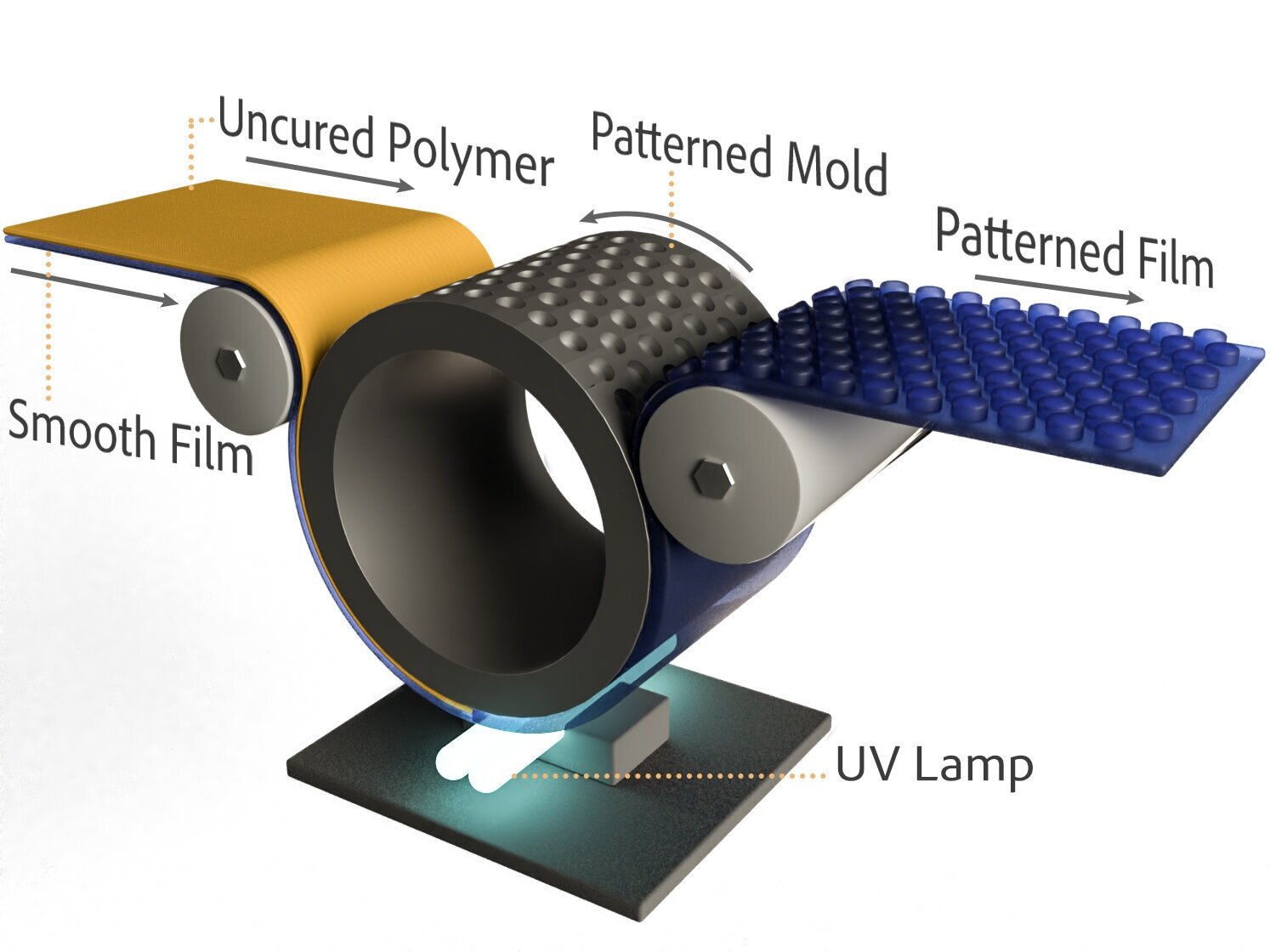
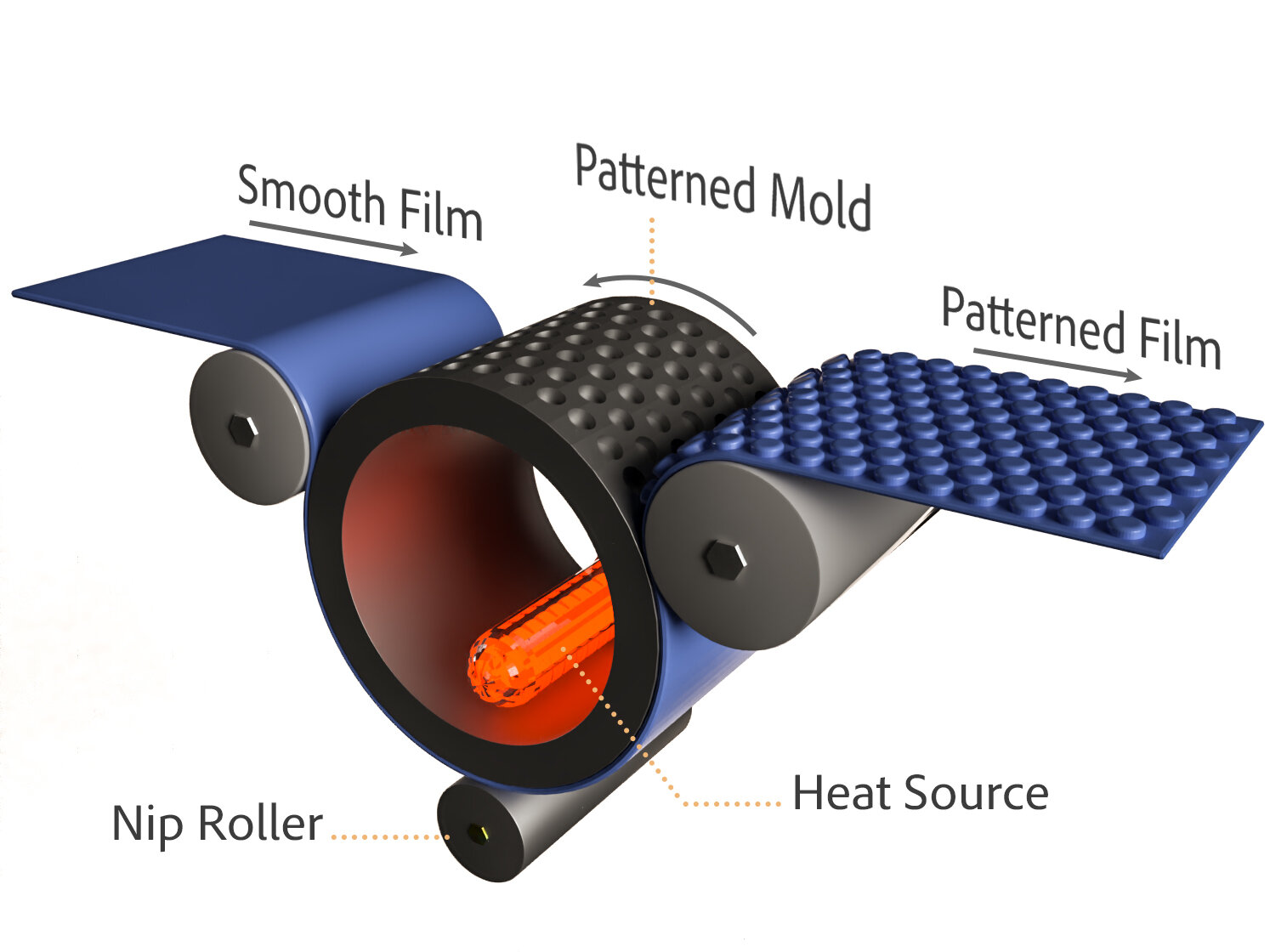
There are two main styles of R2R NIL: photolithography and thermal imprinting. For photolithography, uncured photopolymer is applied to a smooth substrate. The photopolymer-covered substrate is wrapped around the drum mold; while in contact with the mold, the photopolymer is exposed to UV light, curing the polymer. The cured polymer sticks to the backing resulting in a patterned film that is peeled off the mold (Figure 2a). For thermal imprinting, also known as thermal embossing, the patterned drum is heated to raise the temperature of the substrate above the glass transition temperature. Meanwhile, a second “nip” roller applies pressure to the backside of the substrate, causing the softened substrate to fill the pattern on the surface of the drum mold. The web is then cooled and released from the drum (Figure 2b).

Figure 2. Illustrations of a R2R photolithography setup (a) and a R2R thermal embossing setup (b).

This continuous process allows for replication at rates much faster than step and repeat or “batch” imprinting due to the cycle time required in both thermal and UV processes. A seamless mold also allows the final patterned area in the substrate to be much larger than the pattern created in the mold. These advantages are especially potent in applications that require mass production of films. As an example, if Apple wanted to cover every iPhone sold in 2020 with an antireflective nanopattern, it would take approximately 47 million feet (8,900 miles) of six inch wide substrate. Smart Material Solutions’ advantage is its ability to seamlessly nanopattern cylindrical drum molds for R2R NIL hundreds of times faster than electron-beam lithography using its patented diamond indenting process - nanocoining.

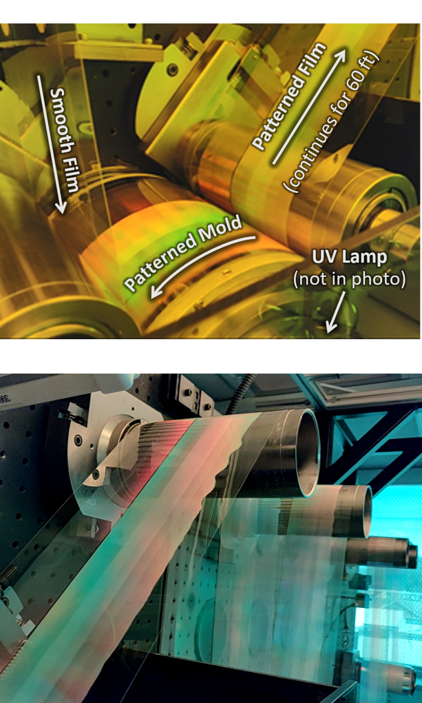
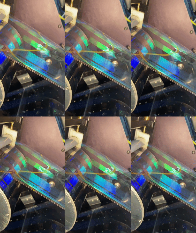
Figure 3. Nanocoined molds from SMS being replicated at UMass Amherst as part of an NSF Phase II SBIR 1738387 (a) and at MicroContinuum, Inc. as part of our current Army Phase II STTR W15QKN19C0044 (b).

Keeping clean on the Moon: Nanostructured surfaces to reduce lunar dust adhesion

Smart Material Solutions has been working for five years on scaling so-called “functional surface textures.” In May 2021, we partnered with Prof. Chih-Hao Chang of the University of Texas, Austin NASCENT Center and won a NASA-funded Small Business Innovation Research (SBIR) contract to adapt our technology for a new functionality: dust mitigation on spacecraft components on the moon.

If you’re not a fan of dust, the Moon is not the place for you. The moon has no liquid water, wind, weather, or even atmosphere. Everything we see on the surface is the result of meteor impacts, which all at once melt, turn to glass, and then shatter the minerals on the surface. The result is an extremely abrasive, microscopic, electrically charged dust that sticks to everything and is never worn down by the weather - even after billions of years! Lunar dust wreaked havoc during the Apollo Missions, with so much being tracked into the Lunar Module that it created haze in the cabin. With return to the moon via Artemis inevitable, the problem has resurfaced as a NASA priority.

Nanostructures on a surface dramatically affect how that surface interacts with the environment. For instance, texturing a surface with nanoscale features can make the surface self-cleaning via the lotus effect or decrease the adhesion of dust to a surface. This provides an opportunity for a passive solution to the dust problem. Passive solutions require no power or increase in payload mass, unlike, for example, an air spray, windshield wiper, vibrating panel, electrodynamic dust shield, or other proposed “active” solutions. 

Nanostructures essentially place the tiny micro-dust particles on a bed of nails, as shown in Figure 1. This reduces the contact area and the microscale adhesion forces, such as Van der Waals forces. The spacing between the nanostructures is important. It determines whether a dust particle will sit on top of multiple features, as desired, or whether it will stick between them, effectively making the problem worse.

Figure 1 - Large dust particles (left) sit on top of the features of a textured surface (desirable), while small dust particles (right) can fall in between the features (undesirable).

Lunar dust consists of a wide array of particles ranging from 1 μm to 100 μm in size. Single-digit micron-scale surface features may help reduce the adhesion of 10 μm particles or larger but become clogged over time with the smaller 1 μm particles. So the first goal of surface design is to reduce the spacing between the surface features as much as possible.

Another factor that impacts adhesion is the radius of curvature and material properties of the two bodies being attracted. In general, softer surface materials with larger features will have a larger contact area and thus larger adhesion force, as shown in Figure 2. So given the option, the goal is to make the individual features as sharp as possible to limit contact area.

Figure 2 - Sharper features (right) have a smaller contact area and thus reduced adhesion.

These geometric properties combine with material properties like hardness, surface energy, and electrical conductivity to determine a surface's passive affinity for dust. Unfortunately, due to the harsh realities of the lunar environment, including unfettered UV exposure and 200 degree temperature swings, the materials available for texturing are limited and typically so robust that they’re hard to pattern through the typical thermal embossing or UV curing processes. Solving this problem, at scale, is the goal of SMS’s NASA-sponsored SBIR Project. Figure 3 shows exciting preliminary results from this project.

Figure 3 - Video comparing the dust-mitigating properties of a smooth and a nanopatterned film. The two films were covered in Lunar dust simulant and tilted so that gravity could remove the bulk of the dust. After tilting, the smooth film remains covered in dust, whereas the nanopatterned film is largely free of dust.

For updates on this project and others, sign up for our newsletter!

Newsletter - July 13, 2021

Smart Material Solutions is excited to make two big announcements - both with a focus on keeping clean! In May, we started an SBIR with NASA to create dust-mitigating surfaces in support of NASA's return to the moon. To go along with that, we recently completed our own in-house cleanroom at SMS! As usual, we're open to discussing our work and forming new partnerships as we develop new application areas for our large-area nanoimprint molds.

New Cleanroom Facilities

SMS employees took a break from their normal experiments to construct a new cleanroom that houses the nanocoining pilot line and nanoimprint lithography (NIL) equipment. This custom-designed facility offers superior temperature control and dust suppression. Check out a timelapse of the construction below!

NASA Phase I SBIR: Dust-Mitigating Surfaces

SMS was awarded NASA Phase I SBIR to create dust-mitigating surfaces in space-grade materials using nanocoining. We will collaborate with Professor Chih-Hao Chang at UT Austin to create nanopatterns and test their ability to minimize dust adhesion via the lotus effect.

polymer.png

Newsletter - May 21, 2021

Army Phase II SBIR Award: R2R fabrication of plasmonic absorbers

SMS was awarded an Army Phase II SBIR for the R2R fabrication of plasmonic absorbers. During the phase I project, SMS teamed with Professor Mark Mirotznik of the University of Delaware to design and fabricate a large-area plasmonic absorber using nanocoining and nanoimprint lithography (see photo and SEM image). In phase II, SMS will work with Professor Mirotznik and MicroContinuum, Inc. to scale up the process using R2R fabrication. This project will demonstrate the promise of nanocoining for the scalable manufacturing of patterned metal films for plasmonic devices, transparent conducting metal mesh films, and wire grid polarizers.

ArmySC.png

Article on R2R Fabrication Published in Nanotechnology

SMS collaborated with the Center for Hierarchical Manufacturing (CHM) at the University of Massachusetts at Amherst to nanopattern more than 60 feet of polymer film using a seamless cylindrical mold created with nanocoining (see photo and SEM image). This work, which was the first demonstration of R2R fabrication with our drum molds, was published in the journal Nanotechnology.

R2R.png

Newsletter - October 15, 2020

Our first product: Low-cost master molds for nanoimprint lithography!

We’re excited to announce our first products, which are now available on our website.

flat mold.jpg

Flexible micro- and nanopatterned shims for applications including:

  • Anti-reflective films

  • Optical arrays

  • Enhanced wetting

  • Etch templates

Form factors:

  • Standard foil shims of 25 mm x 25 mm.

  • Custom development of shims, seamless sleeves, and solid cylinders up to 160 mm x 160 mm.

Patterns:

  • Standard patterns with 2 µm and 3 µm pitch and 0.5 aspect ratio (height/pitch) on a square grid. More patterns including 1 µm and 600 nm pitch coming soon.

  • Custom development of close-packed arrays, novel patterns, and feature pitches from 200 nm – 6 µm