Roll-to-roll, also referred to as reel to reel, technology began in the 1800’s as a way to mass produce newspapers and photographs. Since then it has been incorporated into the production of goods ranging from food packaging to flexible electronics, and more recently in emerging nanotechnology applications. Smart Material Solutions primary mission is to supply the seamless nanopatterned drum molds needed for roll-to-roll nanoimprint lithography (R2R NIL).
R2R manufacturing is a method of fabrication in which a continuously moving, flexible substrate is processed. The processing looks different depending on the application but can include printing, patterning, coating, or lamination. In all cases, the substrate starts wound on one roll, undergoes the processing steps, and then the finished product is wound onto a second roll (Figure 1). Nanoimprint lithography (NIL) is the process of replicating nanoscale patterns from a mold into another material. When combined, R2R processing and NIL result in a high-speed, continuous process to produce large areas of nanopatterned surfaces.
Figure 1. R2R production diagram, where the processing steps are represented by block S1 through S5 and a tensioning step is represented by roller T.
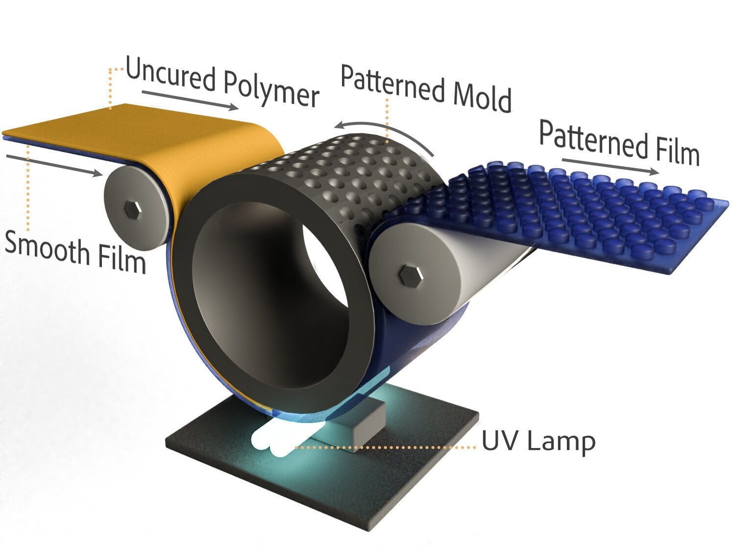
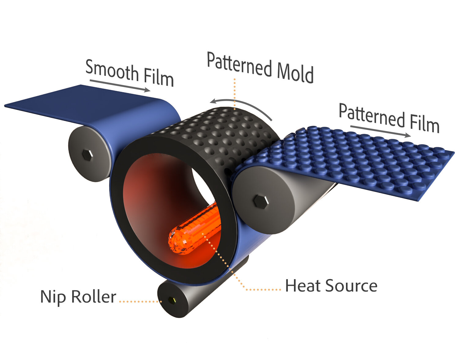
There are two main styles of R2R NIL: photolithography and thermal imprinting. For photolithography, uncured photopolymer is applied to a smooth substrate. The photopolymer-covered substrate is wrapped around the drum mold; while in contact with the mold, the photopolymer is exposed to UV light, curing the polymer. The cured polymer sticks to the backing resulting in a patterned film that is peeled off the mold (Figure 2a). For thermal imprinting, also known as thermal embossing, the patterned drum is heated to raise the temperature of the substrate above the glass transition temperature. Meanwhile, a second “nip” roller applies pressure to the backside of the substrate, causing the softened substrate to fill the pattern on the surface of the drum mold. The web is then cooled and released from the drum (Figure 2b).
Figure 2. Illustrations of a R2R photolithography setup (a) and a R2R thermal embossing setup (b).
This continuous process allows for replication at rates much faster than step and repeat or “batch” imprinting due to the cycle time required in both thermal and UV processes. A seamless mold also allows the final patterned area in the substrate to be much larger than the pattern created in the mold. These advantages are especially potent in applications that require mass production of films. As an example, if Apple wanted to cover every iPhone sold in 2020 with an antireflective nanopattern, it would take approximately 47 million feet (8,900 miles) of six inch wide substrate. Smart Material Solutions’ advantage is its ability to seamlessly nanopattern cylindrical drum molds for R2R NIL hundreds of times faster than electron-beam lithography using its patented diamond indenting process - nanocoining.
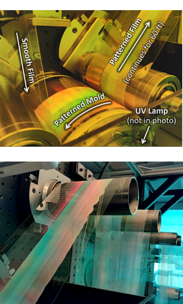
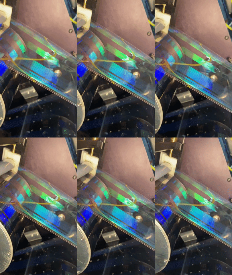
Figure 3. Nanocoined molds from SMS being replicated at UMass Amherst as part of an NSF Phase II SBIR 1738387 (a) and at MicroContinuum, Inc. as part of our current Army Phase II STTR W15QKN19C0044 (b).


