Looking into the Nanoworld
I’m going to ask the question that bothered me to no end while I was in grade school. If the 100x objective will allow me to see this amoeba, why can’t we just put on a 1,000,000x objective so I can see its individual atoms?! It turns out, no matter how petulant a nerd I was, there was a very good reason that my 6th grade teacher couldn’t produce a live view of a proton on the benchtop visible microscope.
It’s not that my school’s budget didn’t include a line for the 1,000,000x objective. There is a fundamental limit to how small of a thing you can see with visible light. This limit exists because light, by its nature, is a wave with a given wavelength. Roughly speaking, you cannot see anything that is smaller than half the wavelength you’re using to observe (see the last section for details). In the case of humans, our eyes can see light that ranges between 380 nm (violet) and 750 nm (red), known as the “visible band.” This means, no matter how much we zoom in, the human eye is not going to see anything smaller than 200 nm, even with the best visible light microscopes.
Defying the Limits of the Human Eye
To look smaller, you need to reduce the wavelength of the light or wave you’re using to observe. Figure 1 shows the range of waves on the electromagnetic spectrum, including the visible light band between 380 and 750 nm and common objects overlaid for scale. Longer wavelengths include infrared light that is used in night vision and thermal imaging, microwaves that can heat your food, and radio waves, while shorter wavelengths include ultraviolet light, X-rays, and gamma rays.
Figure 1. Electromagnetic spectrum.
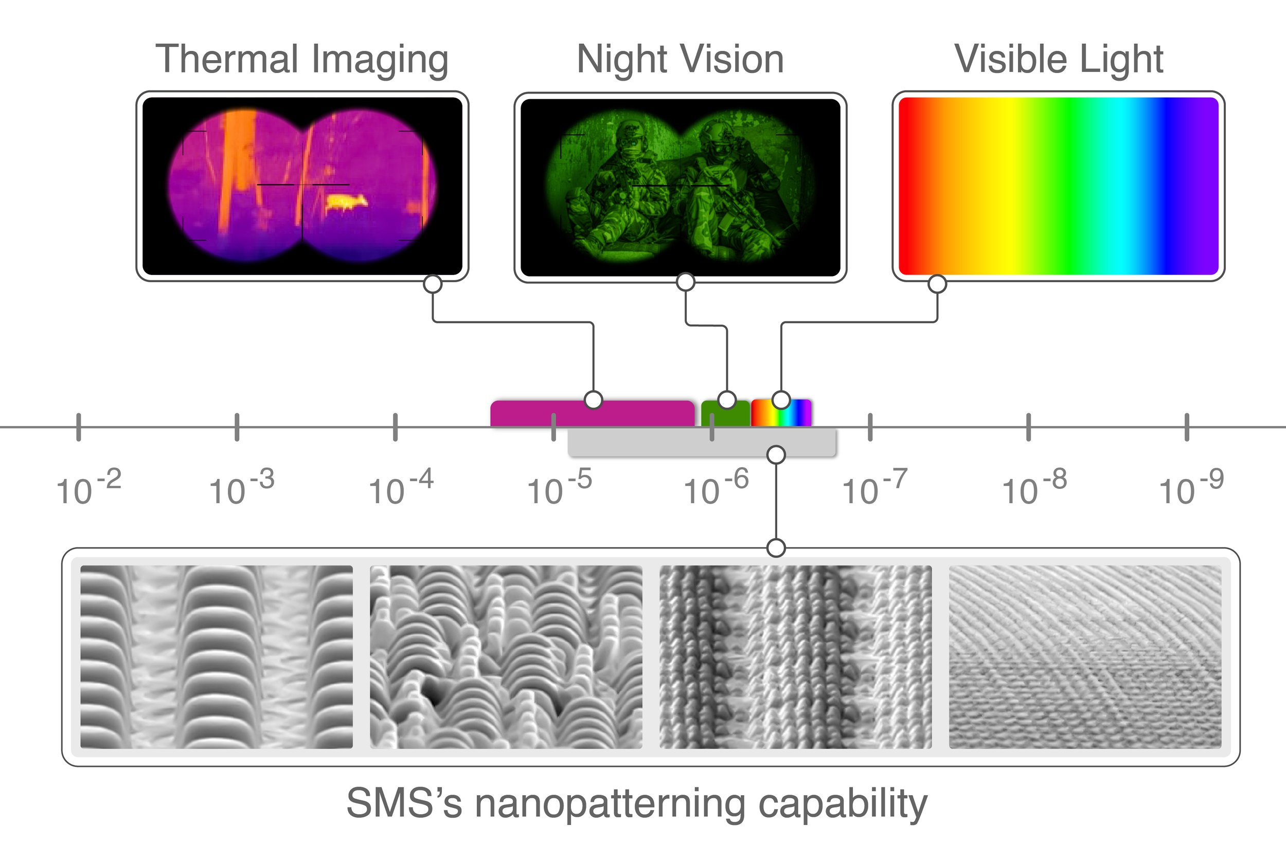
Figure 2 zooms in on the wavelength ranges used by thermal imaging, night vision, and visible light, along with the range of features sizes that SMS can make and use to manipulate the electromagnetic spectrum.
Figure 2. Subset of the electromagnetic spectrum.
Viewing objects that are smaller than visible wavelengths can be done by either slowing down visible light to reduce its wavelength or by using shorter wavelengths to begin with. However, using wavelengths beyond the visible spectrum becomes understandably tricky, because in order for us to see what the shorter wavelength light sees, we need to sense it with a detector then convert it back into a ‘false image’, typically by a computer. The common types of microscopy are described below, and their viewing ranges are overlaid on Figure 1 as well.
Figure 3. Optical microscopy image showing an onion’s cell walls.
Optical Microscopy, also known as light microscopy or visible microscopy, is the most commonly used form of microscopy. This simple, low-cost method uses visible light to observe specimens and provides valuable insights into their structures. Techniques like brightfield and darkfield microscopy offer versatility in analyzing a wide range of samples from cells, tissues, and microorganisms to microstructures in engineered materials (Figure 3). However, optical microscopes cannot resolve nanoscale objects that are substantially smaller than the visible light wavelengths they use to probe the sample.
Oil Immersion Microscopy is an extension of visible microscopy that enhances resolution by making the observations in a droplet of oil, where the speed and therefore the wavelength of ‘visible’ light is reduced. To achieve this, a special immersion oil is placed between the objective and the sample. However, this requires careful handling methods and cleanup, and the observation often destroys or contaminates your sample.
Scanning Electron Microscopy (SEM) is a powerful technique that uses a focused beam of electrons to obtain high-resolution images of a sample's surface. Much like a photon of light, electrons also have a wavelength that depends on their energy. The energy of electrons in a SEM allows them to probe nanoscale features that are much smaller than what is observable with optical microscopy (Figure 4). By scanning the surface with the electron beam, SEM creates detailed images, revealing the topography and surface features of the specimen with exceptional depth of field (Figure 5). Most traditional SEMs require electrically conductive samples and vacuum conditions that can affect the sample's natural state of biological samples, but specially designed environmental SEMs can image non-conductive and even wet samples in a gaseous environment.
Figure 4: Sub-micron details of a Blue Morpho butterfly wing.
Figure 5: Wide view SEM of a Blue Morpho butterfly wing showing depth of field.
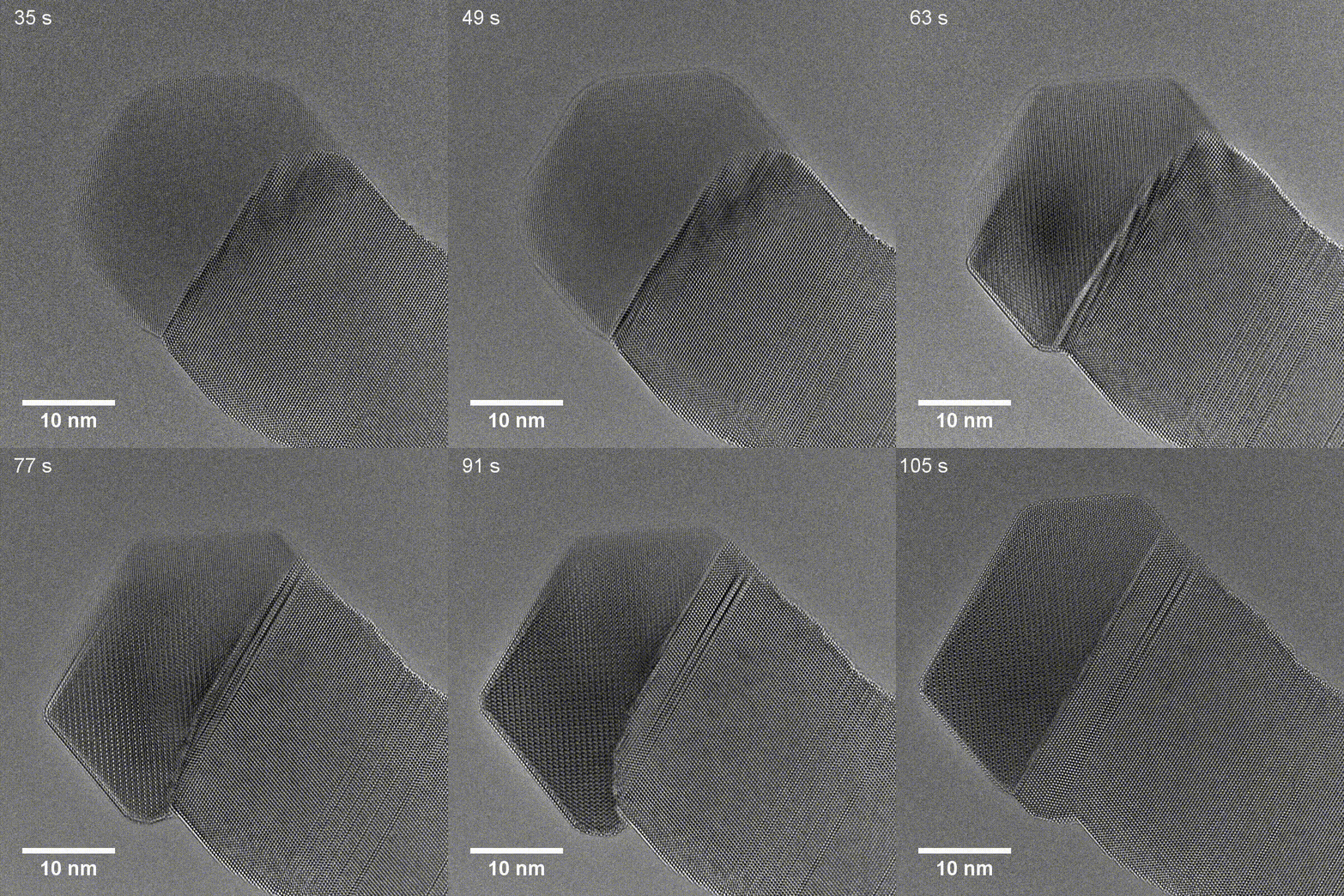
Figure 6. TEM of GaP nanowire growth using a Cu seed taken by Tianyi Hu for his article in Small Structures.
Transmission Electron Microscopy (TEM) uses a beam of high-energy electrons that passes through thin sections of a sample to create a highly detailed image of the specimen's internal features. TEM enables scientists to visualize fine details such as individual atoms and lattice structures like those seen in the GaP nanowire and Cu seed in Figure 6, but the technique requires specialized sample preparation like thin sectioning, which can be time-consuming and introduce artifacts. Additionally, high vacuum conditions can pose limitations for certain types of samples.
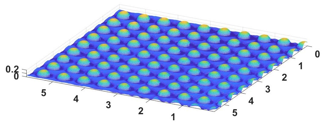
Figure 7. AFM of polymer nanofeatures created by SMS with dimensions labeled in microns.
Atomic Force Microscopy (AFM) is different, as it does not use light to ‘probe’ the surface being measured. Instead, AFM measures the interaction forces between a sharp probe and a sample's surface. Since the probe point can have a radius as small as a few nanometers, it can resolve extremely fine features. As the probe scans the surface, it records the variations in forces, creating a 3D topographical map that can have atomic-scale resolution (Figure 7). However, AFM operates at a slower speed compared to other techniques and may experience challenges in imaging soft or fragile samples due to probe-sample interactions.
Microscopy in Action at SMS
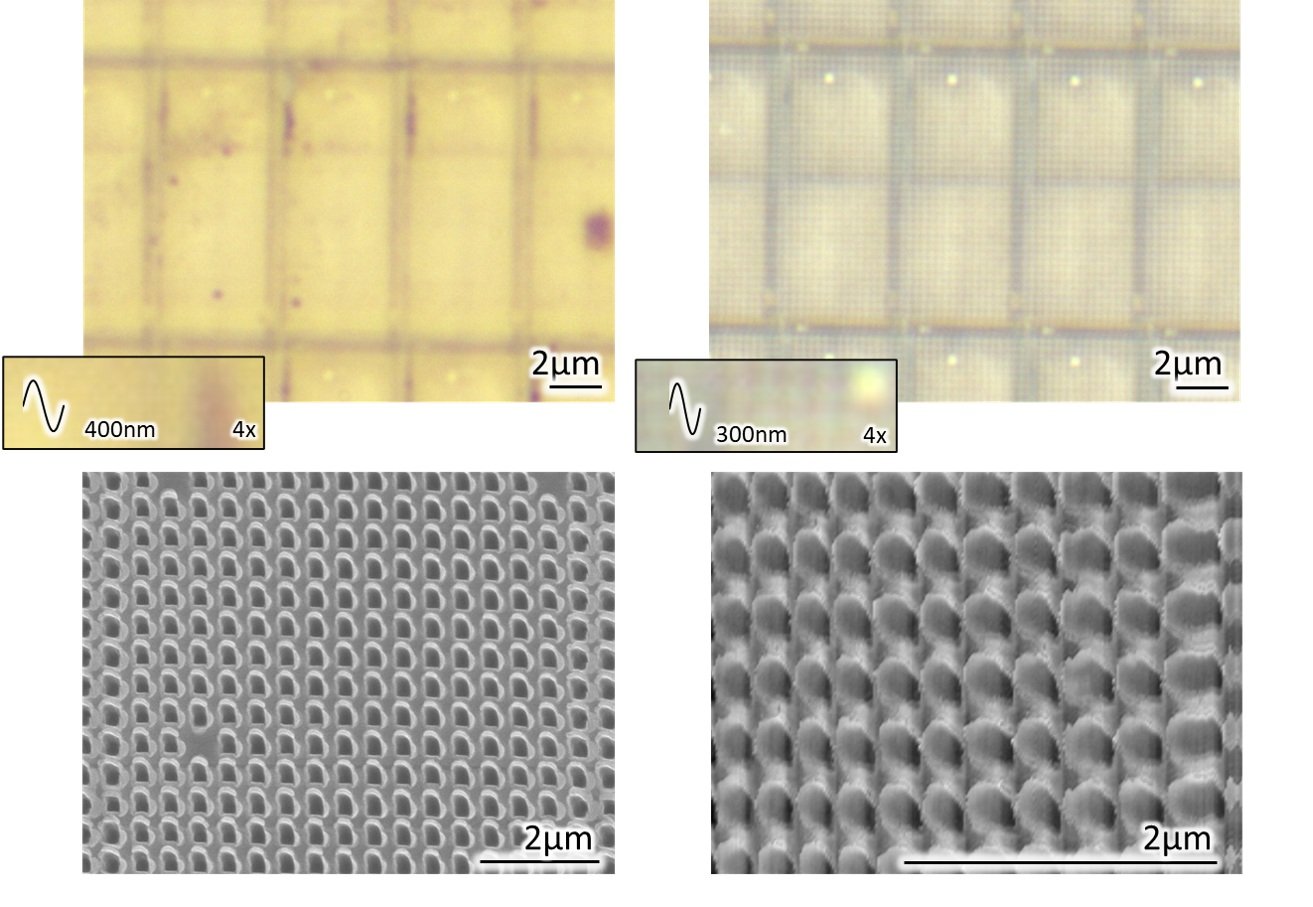
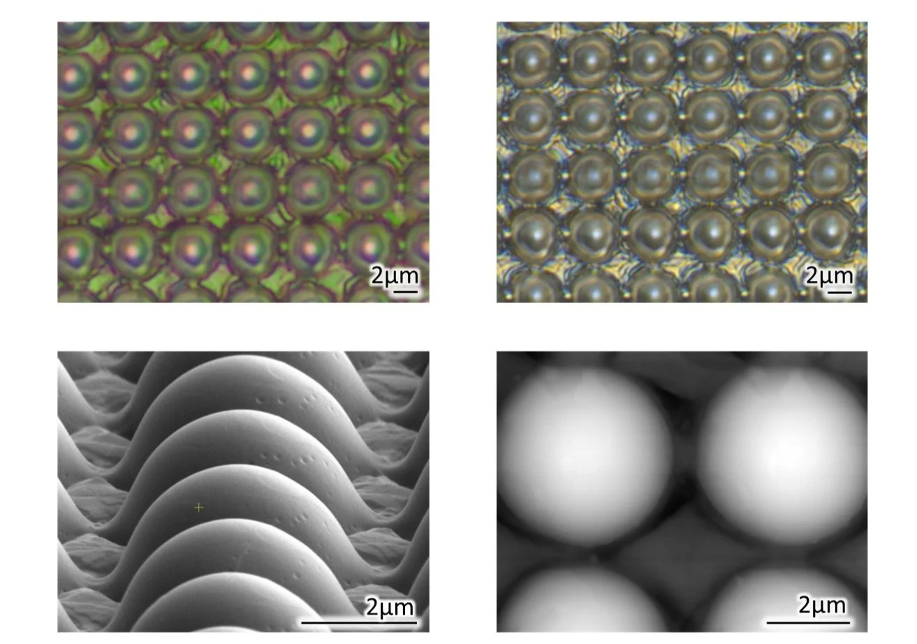
At Smart Material Solutions, we use microscopy every day to measure the functional structured surfaces we fabricate. These surfaces may consist of features that are 5 µm across and therefore observable, with some level of detail, using a visible microscope. Or they may consist of features smaller than 200 nm that require an SEM or AFM to be resolved at all. Figures 8 and 9 show arrays of similarly shaped features with center-to-center distances of 300 nm and 5 µm, respectively, as observed by several different microscopy techniques. Interestingly, the 300 nm features become visible with oil immersion, in the top right image!
Figure 8. A 300nm mold imaged using visible microscopy (top left), oil immersion microscopy (top right), SEM (bottom left) and AFM (bottom right). For the visible and oil immersion micrographs, the imaging wavelength is overlaid on a magnified view.
Figure 9. A 5µm mold imaged using visible microscopy (top left), oil immersion microscopy (top right), SEM (bottom left) and AFM (bottom right).
Taking Advantage of the Diffraction Limit
In microscopy, the diffraction limit is the minimum resolvable distance, originally defined by Ernst Abbe as:
|
D = |
λ
2*n*sin(θ)
|
− |
λ
2*NA
|
|
Where n is the index of refraction of the medium, e.g. air, and theta is the half angle of the light converging from the objective. n*sin(theta) is known as the numerical aperture, NA, of the optical system, which can be up to ~1.6 in modern, high-end visible microscopes.
This limit is almost always a nuisance that must be overcome with a more complex and expensive instrument. However, at SMS, we specialize in using this effect to our advantage. For example, leveraging the moth-eye effect, we make features so small that they appear invisible to the human eye, but nevertheless reduce reflections, mitigate dust adhesion, or help kill or shed microbes. Further, we’ve begun building multilayer structures comprised of different materials - arranged in sub-wavelength arrays - that exhibit properties unattainable by any naturally occurring materials. These are known as metamaterials, and they’re the future.


