Machinists shape parts using tools like milling machines, which cut away material with a spinning bit like the one shown in Figure 1A. Milling on the nanoscale requires a nanoscale tool like a focused ion beam (FIB), which can be as small as a few nanometers in diameter. When an ion beam strikes a surface, the incoming ions knock out atoms, removing material in the beam’s path (Figure 1B).
Figure 1: Illustration of milling with a milling machine (A) and FIB milling on the nanoscale (B).
Figure 2: Electron microscopy image of examples of FIB milling and deposition.
The FIB-milling process can also be modified to deposit material instead of removing it, enabling FIB deposition of complex 3D nanostructures in a process that is similar to some 3D-printing techniques (Figure 2). The nanoscale patterns created with FIB milling (also known as FIB machining) and FIB deposition have applications ranging from solar panels to antimicrobial surfaces.
FIB Milling
FIB milling uses an ion beam to remove material in its path. The ion beam often consists of gallium ions, but other ions including xenon, argon, nitrogen, and oxygen can also be used.
Figure 3: FIB milling process viewed from the atomic scale.
Let’s consider what happens at the atomic scale when a beam of gallium ions hits a piece of gold. As illustrated in Figure 3, gallium ions that collide with the gold will knock out some of the gold atoms in a process known as sputtering. A fraction of the sputtered gold atoms may then redeposit on another part of the gold piece. Some of the gallium ions will rebound away from the gold surface, while others become implanted inside the gold. The end result is the removal of gold atoms from the place of impact.
The more time the ion beam is held at a particular position, the more material it will remove from that position. Thus, scientists can create complex nanostructures by controlling how long the beam sits over each position of a sample. This is unlike a milling machine, that effectively subtracts the exact geometry of the cutting tool from the workpiece within one revolution of the tool, then stops cutting, no matter how long the tool dwells.
Further, a FIB removes more material near the beam center and less material at the beam edges. This occurs because a FIB contains more ions near the center of the beam and fewer ions near the beam edges as illustrated in Figure 4.
Figure 4: Plot illustrating distribution of ions in a FIB (left), and illustration of the cross section of a material that has been FIB milled at one position (right).
Another complexity arises from the dependence of sputtering efficiency on incidence angle. Figure 5 shows how sputtering can be inefficient when the FIB is perpendicular to a surface, because the sputtered ions must exit the sample in the opposite direction of the incoming ion beam. Tilting the sample will increase sputtering efficiency since sputtered ions do not have to change direction so drastically to leave the sample. This leads to an angle-dependence of the sputtering yield, or the number of sputter atoms per incoming ion. A surface that has been nanostructured with a FIB beam will have a variety of angles between the local surface and the incoming FIB beam, meaning that different points in a material will sputter different amounts of material when exposed to the same ion dose. Precise control over the shape of a FIB-milled nanostructure therefore requires compensation for both the angle-dependent sputtering efficiency and the shape of the ion beam.
Figure 5: Angle dependence of sputter yield. Inserts illustrate sputtering with a FIB that is perpendicular to the sputtered surface and incident on a tilted surface.
FIB Deposition
A FIB can also be used to deposit material if certain precursor molecules are introduced into the system. Properly chosen molecules will adsorb onto the surface of the material. When the FIB scans over these adsorbed molecules, it will drive a chemical reaction that solidifies these materials as illustrated in Figure 6. Materials that are commonly deposited by FIB include platinum, diamond-like carbon, tungsten, and silica. FIB-deposition can be used to repair circuits in microchips, protect underlying features, or to make cool-looking nanostructures like those in Figure 7. Although this blog discusses FIB-deposition techniques, electron beams like those in electron microscopes can also drive chemical reactions that solidify precursor molecules.
Figure 6: During FIB deposition, a FIB drives a chemical reaction that solidifies precursors introduced into the system.
Figure 7: Examples of FIB-deposited nanostructures including nanoscale models of a bacteriophage and the leaning tower of Pisa. Nanostructures created by Reo Kometani and Sunao Ishihara.
FIB Patterning at Smart Material Solutions
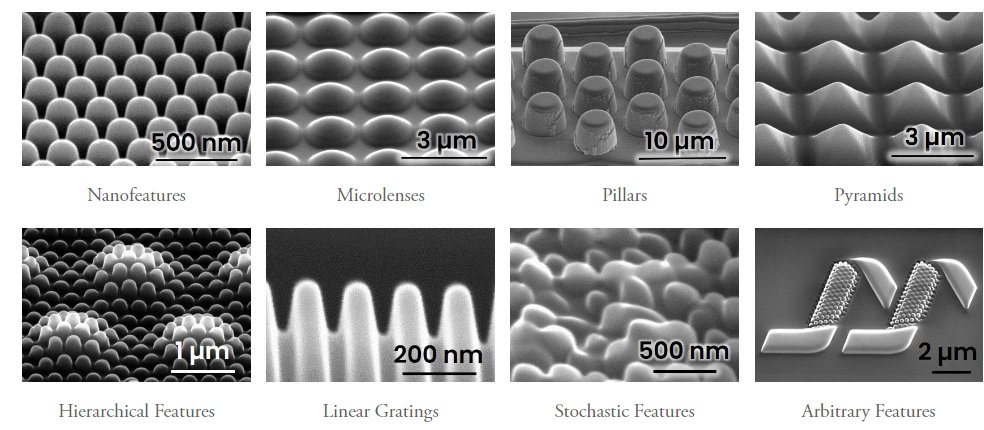
Smart Material Solutions often uses a FIB to nanopattern the diamonds it uses for its patented nanocoining process to create seamless cylindrical molds for R2R nanoimprint lithography. Figure 8 shows some of SMS’s FIB-milled nanostructures for a variety of applications including dust-mitigating surfaces, light-trapping films to increase the efficiency of solar panels, and anti-reflective motheye films. One of our employees, Nichole Scott, even used the FIB to engrave the side of her engagement ring as shown in the video in Figure 9.
Figure 8: Some of the nanostructures FIB-milled into diamond at North Carolina State University’s Analytical Instrumentation Facility (AIF).
Figure 9: Video showing FIB-patterned engagement ring.


